Course "Architecture of Multi-Processor Systems"
TP3: Internal architecture of the cache controller
(pirouz.bazargan-sabet@…)
A. Objectives
In this lab, we analyze the internal architecture of an L1 cache controller containing an instruction cache and a data cache. The two caches are independent, but share the same PIBUS access port. Recall that in a set associative cache, the set of all cache lines is partitioned into NSET families according to the value of the SET field of the address. Each family is assigned a set of equivalent NWAY cells. For a family identified by a SET number, the cells are differentiated by a WAY number. The total number of cells is therefore equal to NSET * NWAY. All lines of a family compete for the NWAY cells allocated to the family. In a direct match cache, NWAY = 1, so a cache line can only be stored in one cache bin. In a fully associative cache, any cache line can be stored in any bin, so there is only one family and NSET = 1.
The 32-bit address is split as follows:
| TAG | SET | BYTE |
- The BYTE field designates a byte in a line
- The SET field defines a family number
- The TAG field identifies a particular line in a family
The memory write strategy is a "write-through" strategy: any write request issued by the processor results in an immediate write to memory (as soon as the cache controller can access the bus). The cache is only updated if the address corresponds to data in the cache. A posted write buffer avoids freezing the processor during write instructions (sw or sb instructions), as long as there are not too many consecutive writes.
B. Hardware architecture

The architecture of the system considered in this practical is identical to that of practical 2. It consists of a single MIPS32 programmable processor with caches, RAM, ROM, and a TTY terminal. Create a working directory tp3, and copy in this directory the two files tp2_top.cpp and tp2.desc already used in TP2.
In TP3, two direct-match caches are used, each with a capacity of 128 bytes, and cache lines with a width of 4 words of 32 bits. Start by modifying the values of the parameters defining the characteristics of the caches in the file tp2_top.cpp and then generate the simulator.
C. Software application
The archive multi_tp3.tgz contains the files you will need: you will find in the 'soft' directory the file 'main.s' (user program in assembler), the file reset. s (boot code), the files seg.ld, sys.ld and app.ld (allowing to control the link edition), the file config.h, and a file Makefile allowing to launch the generation of the binary code. Uncompress this archive in the tp3 directory.
The program executed in TP2 was written in C language. In this TP3, the main program contained in the file main.s is written in assembler to facilitate the control of the values of the addresses of the code and the data.
This program performs the vector addition: C = A + B. The 3 vectors A, B and C have 20 components each. These vectors are represented in memory by arrays of integers. Before entering the loop that performs the addition, the address of the element A[0] is loaded into register $8.
Check that the segment addresses defined in the file seg.ld (for software) are consistent with the values defined in the file tp2_top.cpp (for hardware).
Open the main.s file to answer the following questions:
Question C1: What is the address of the first statement in the main function? What is the address of the first instruction of the loop (instruction corresponding to the label loop)?
Question C2: What are the base addresses of the three arrays A, B, C?
Question C3: Why is the instruction sw placed after the instruction bne (end of loop test)?
Question C4: What is the number of cycles required to execute one iteration of the loop, assuming all instructions and data are in the cache (no MISS).
D. How the instruction cache works
We will now analyse the behaviour of the instruction cache. That is to say, we will try to predict the evolution of the contents of the cache during the execution of the program.
Question D1 : On how many bits are the three fields BYTE, SET, and TAG of a 32-bit address coded? What are their values for address 0x00400000 (corresponding to the first instruction of the program?)
Question D2: Show the contents of the instruction cache at the end of the first iteration of the loop in the table below. Which instructions triggered a MISS on the instruction cache to reach this state?
| TAG | V | WORD3 | WORD2 | WORD1 | WORD0 |
| 0 | |||||
| 0 | |||||
| 0 | |||||
| 0 | |||||
| 0 | |||||
| 0 | |||||
| 0 | |||||
| 0 |
For the 4 columns on the right, each cell of the table contains a 32-bit word.
Question D3: What is the content of the instruction cache at the end of the 20th iteration? Calculate approximately the MISS rate during the complete execution of the program (we do not take into account what happens during the boot sequence and during the message display).
We are now interested in the automaton that controls the instruction cache. Processing a MISS instruction requires the cooperation of two automata: When the ICACHE_FSM automaton detects a MISS condition, or a non-cacheable address, it calls on the PIBUS_FSM automaton to perform the transaction on the PIBUS following the PIBUS protocol.
In the event of a MISS, the ICACHE_FSM stores the address of the missing line in a register, then enters the MISS_SELECT state to select the box where the missing line will be stored, then enters the MISS_WAIT state, where it waits for the PIBUS_FSM to finish writing all the words of the missing line into the buffer register. Finally, the ICACHE_FSM updates the instruction cache in the MISS_UPDT state and then returns to the IDLE state. The ICACHE_FSM is capable of handling non-cacheable instruction read requests (UNC_WAIT and UNC_GO states), and must also report any addressing errors reported by the PIBUS_FSM to the processor (ERROR state).
Question D4: For which type of cache is the MISS_SELECT state necessary?
Question D5: Complete the graph of the ICACHE_FSM automaton below, attaching to each transition its crossing condition. The transition conditions depend on the following Boolean signals:
- IREQ: the processor issues an instruction request,
- IUNC: the address corresponds to a non-cached segment,
- IMISS: the instruction cache does MISS,
- VALID : the PIBUS automaton signals that the answer is available,
- ERROR: the PIBUS automaton reports that the response is an error.
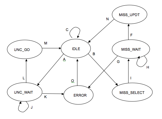
Question D6: What state is this PLC forced into when the RESETN signal is activated? What should be the other effect of the RESETN signal on the instruction cache?
Note: It is not forbidden to consult the simulation model contained in the file pibus_mips32_xcache.cpp to do reverse engineering and try to extract the structure of the automata. We remind you that these models are stored in the directory :
/users/outil/soc/soclib-lip6/pibus
E. How the data cache works
We will now analyse the behaviour of the data cache.
There is no data read (no lw or lb instruction) in the boot code contained in the reset.s file. The data cache is therefore initially empty (i.e. the 8 boxes have invalid contents).
Question E1: What are the values of the three fields BYTE, SET, and TAG for the addresses of elements A[0] and B[0] in the two arrays? Give the contents of the data cache at the end of the first iteration of the loop, specifying which instructions cause a MISS on the data cache and thus a processor freeze.
| TAG | V | WORD3 | WORD2 | WORD1 | WORD0 |
| 0 | |||||
| 0 | |||||
| 0 | |||||
| 0 | |||||
| 0 | |||||
| 0 | |||||
| 0 | |||||
| 0 |
For the 4 columns on the right, each cell of the table contains a 32-bit word.
Question E2: Calculate the MISS rate on the data cache for the complete execution of the 20 iterations of this loop. Give the contents of the data cache at the end of the 20th iteration of the loop.
The data cache controller automaton is very similar to the instruction cache controller automaton. We must add the two states for handling writes: the WRITE_UPDT state corresponds to updating the cache in the event of a write that HITs the cache. The WRITE_REQ state corresponds to the recording of the write request in the write buffer.
Question E3: Complete the graph of this automaton, attaching to each transition its crossing condition. These conditions depend on the following Boolean signals:
- DREQ: the processor sends a data request,
- WRITE: this is a write request,
- DMISS: the data cache does MISS,
- DUNC: the address corresponds to a non-cached segment,
- WOK: the write buffer is not full,
- VALID : the PIBUS automaton reports that the response is available.
- ERROR: the PIBUS automaton reports that the response is an error.
Note that the transitions out of the WRITE_REQ state are not represented on the graph below. These transitions are covered in the next question.

In order to be able to process write bursts efficiently, the processor requests are taken into account in the IDLE state and the WRITE_REQ state in the same way. This means that the successor states of the WRITE_REQ state are the same as the successor states of the IDLE state.
Question E4: The Boolean expressions associated with the exit transitions of the WRITE_REQ state are very similar to the Boolean expressions associated with the exit transitions of the IDLE state. What is the difference?
F. Accessing the PIBUS
The PIBUS_FSM can be considered as a server that responds to requests from three clients, which are the ICACHE_FSM, the DCACHE_FSM and the WBUF post buffer. It can generate six types of transactions on the bus corresponding to the following six events (the conditional write instruction SC is used for synchronisation, and will be analysed in the rest of the course):
- The WBUF buffer is non-empty, and requests a WRITE transaction (write a word).
- the DCACHE_FSM automaton requests a SC transaction (conditional writing of a word).
- the DCACHE_FSM automaton requests a DUNC transaction (read a non-cacheable word).
- the DCACHE_FSM automaton requests a DMISS transaction (read a cache line).
- the ICACHE_FSM automaton requests a transaction of type IUNC (read a non-cacheable word).
- the ICACHE_FSM automaton requests an IMISS transaction (read a cache line).
Since several conditions can be true simultaneously, a priority must be defined. The numbering above defines a descending fixed priority order.
Question F1: Why do postings have the highest priority? What is the disadvantage of this choice?
Question F2: What is the mechanism used by the two automata ICACHE_FSM and DCACHE_FSM to transmit a read request to the automaton PIBUS_FSM? How does the server signal to the clients that the request has been answered? In the case of a read request, how does the server notify the client that the data is available?
Question F3: Why does the PIBUS_FSM not need to signal that a write request transmitted by the posted write buffer has actually completed? What is the purpose of the response in the case of a write transaction?
Question F4: Complete the graph of the PIBUS_FSM automaton below, attaching to each transition its crossing condition. These conditions depend on the following signals:
- ROK : The posted write buffer is not empty
- SC : The DCACHE_FSM automaton requests a "conditional write".
- IUNC: The ICACHE_FSM requests a non-cacheable instruction
- IMISS : The ICACHE_FSM automaton requests a cache instruction line
- DUNC : The DCACHE_FSM automaton requests a non-cacheable data
- DMISS : The DCACHE_FSM automaton requests a data cache line
- GNT : The bus is allocated to the PIbusMips32Xcache component
- LAST: A counter set to IDLE state signals that this is the last address of a burst
- ACK: Target response (3 possible values: READY, WAIT, ERROR)

Question F5: Calculate the minimum miss cost on the instruction cache (number of processor freeze cycles in case of a miss). To do this, you will draw explicitly the chronogram describing for each of the two automata, the succession of values stored in the state registers. Same question for the data cache.
Question F6: Calculate the total number of cycles to execute the 20 iterations of the loop in section C, taking into account the freeze cycles due to misses on the instruction cache and data cache. Deduce the value of the CPI (average number of cycles per instruction).
G. Experimentation by simulation
We want to verify by simulation (i.e. experimentation) the calculations made above.
Check that the base addresses of the eight segments in the file tp2_top.cpp agree with the values defined in the file seg.ld.
Verify that the values of the cache parameters defined in the tp2_top.cpp file correspond to direct match caches, each with a capacity of 128 bytes, with a cache line width of 4 words of 32 bits.
Finally, check that the tty segment is declared non-cacheable in the Segment Table.
Generate the sys.bin and app.bin files by running the Makefile in the soft directory. Check that the generated code corresponds to what you expect, in particular with regard to the seg_code and seg_data segments.
Go to the tp3 directory, and run the simulation in trace mode with the -DEBUG option.
The detailed analysis of the trace file will allow you to answer the following questions:
Question G1: At what cycle does the processor execute its first instruction? To which code does this instruction correspond? What is the cost of a MISS on the instruction cache (cost of the MISS = number of processor freeze cycles).
Question G2: At what cycle does the processor branch to the main() function?
Question G3: What is the cost of a MISS on the data cache? At what cycle does the processor complete the execution of the first iteration of the loop? What is the total duration of the first iteration?
Question G4: What is the duration of the second iteration? What is the duration of the third iteration? How do you explain that the MISS cost for iterations 2 and 3 is different from the MISS cost for the first iteration?
Question G5: What is the MISS rate on the data cache at the end of the loop execution? What is the total duration of the main program (not including the execution time of the final message display).
H. Optimization
For this application, the processor freeze cycles due to conflict MISS on the data cache account for more than 2/3 of the execution time. How should the addresses of the arrays in memory be changed to minimize the rate of MISS on the data cache, without changing the hardware architecture and without changing the program structure? Recalculate the total execution time of the program and the average iteration time for this new memory organisation, and check the accuracy of your estimates by simulation.
I. Report
The answers to the above questions must be written in a text editor and this report must be handed in at the beginning of the next lab session. Similarly, the simulator will be checked (in pairs) at the beginning of the next week's practical session.